Платы ПЛИС
Terasic
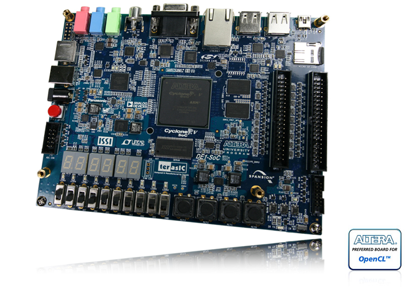
FPGA Device
- Cyclone V SoC 5CSEMA5F31C6 Device
- Dual-core ARM Cortex-A9 (HPS)
- 85K Programmable Logic Elements
- 4,450 Kbits embedded memory
- 6 Fractional PLLs
- 2 Hard Memory Controllers
Switches, Buttons and Indicators
- 4 User Keys (FPGA x4)
- 10 User switches (FPGA x10)
- 11 User LEDs (FPGA x10 ; HPS x 1)
- 2 HPS Reset Buttons (HPS_RST_n and HPS_WARM_RST_n)
- Six 7-segment displays
Документация по работе с платой
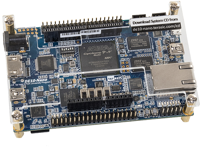
FPGA Device
- Intel Cyclone® V SE 5CSEBA6U23I7NDK device (110K LEs)
- Serial configuration device – EPCS64 (revision B2 or later)
- USB-Blaster II onboard for programming; JTAG Mode
- HDMI TX, compatible with DVI 1.0 and HDCP v1.4
- 2 push-buttons
- 4 slide switches
- 8 green user LEDs
- Three 50MHz clock sources from the clock generator
- Two 40-pin expansion headers
- One Arduino expansion header (Uno R3 compatibility), can be connected with Arduino shields
- One 10-pin Analog input expansion header (shared with Arduino Analog input)
- A/D converter, 4-pin SPI interface with FPGA
Документация по работе с платой
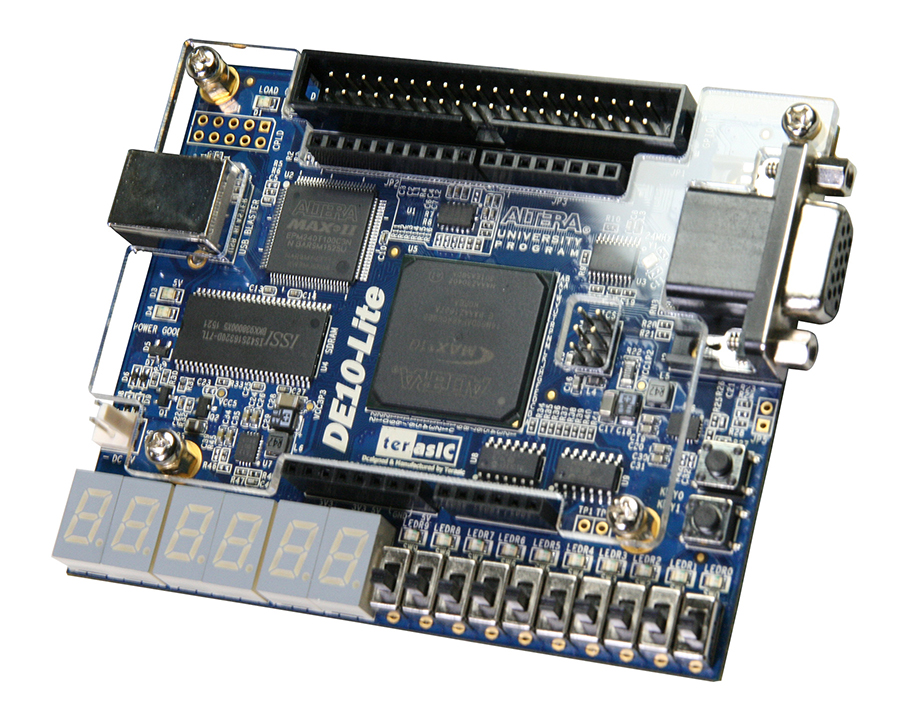
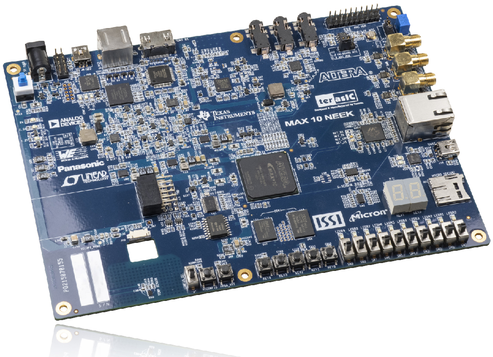
FPGA Device
- MAX 10 10M50DAF484C7G Device
- Integrated dual ADCs, each ADC supports 1 dedicated analog input and 8 dual function pins
- 50K programmable logic elements
- 1,638 Kbit M9K Memory
- 144 18 × 18 Multiplier
- 4 PLLs
Switches/Buttons/LEDs/7-Segment Display
- 10 LEDs
- 10 Slide Switches
- 2 Push Buttons
- Six 7-Segments Display
Документация по работе с платой
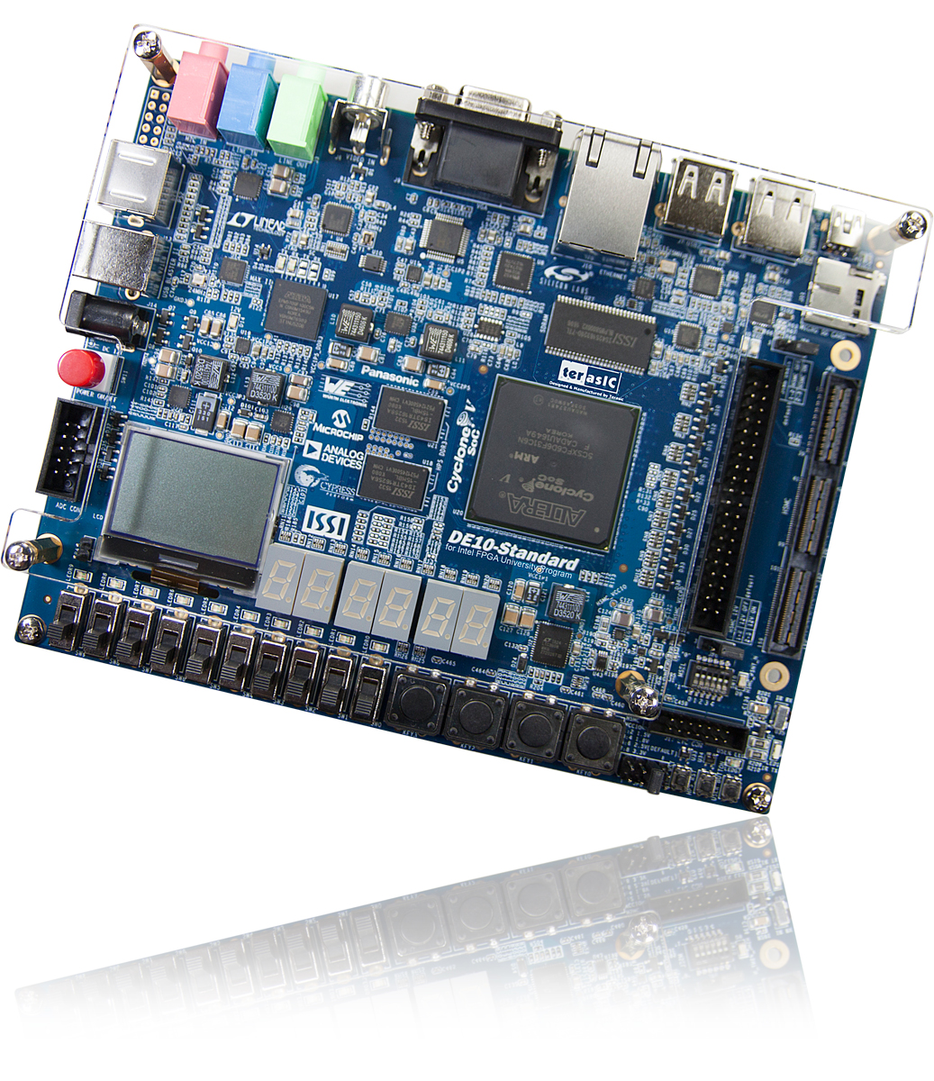
FPGA Device
- Cyclone V SX SoC—5CSXFC6D6F31C6N
- 110K LEs, 41509 ALMs
- 5,761 Kbits embedded memory
- 6 FPGA PLLs and 3 HPS PLLs
- 2 Hard Memory Controllers
Switches, Buttons and Indicators
- 5 User Keys (FPGA x4, HPS x1)
- 10 User Switches (FPGA x10)
- 11 User LEDs (FPGA x10 ; HPS x 1)
- 2 HPS Reset Buttons (HPS_RST_n and HPS_WARM_RST_n)7-Segment Display x6
Документация по работе с платой

Cyclone® IV EP4CE22F17C6N FPGA
- 22,320 Logic elements (LEs)
- 594 Embedded memory (Kbits)
- 66 Embedded 18 x 18 multipliers
- 4 General-purpose PLLs
- 153 Maximum FPGA I/O pins
Документация по работе с платой
FPGA Device
- MAX 10 10M50DAF484C6G Device
- Integrated dual ADCs, each ADC supports 1 dedicated analog input and 8 dual function pins
- 50K programmable logic elements
- 1,638 Kbit M9K Memory
- 5,888 Kbits user flash memory
- 144 18 × 18 Multiplier
- 4 PLLs
- Programming and Configuration
- On-board USB Blaster
- Optional JTAG direct via 10-pin header
- One slide switch for dual boot image selection
Switches, Buttons and LEDs
- Five push-buttons
- Ten slide switches
- Ten red user LEDs
- Two 7-segment displays
Документация по работе с платой
Xilinx

FPGA
- XC7A100T-1CSG324C
I/O Interfaces
- USB-UART for programming and serial communication
- One 10/100 Ethernet
- USB OTG 2.0
- USB-UART bridge
- 12-bit VGA output
- 3-axis accelerometer
- PWM audio output
- Temperature sensor
- PDM microphone
- USB HID Host for mice, keyboards and memory sticks
Switches and LEDs
- 16 Slide switches
- 16 LEDs
- 2 tri-color LEDs
- 5 Push-buttons
Документация по работе с платой
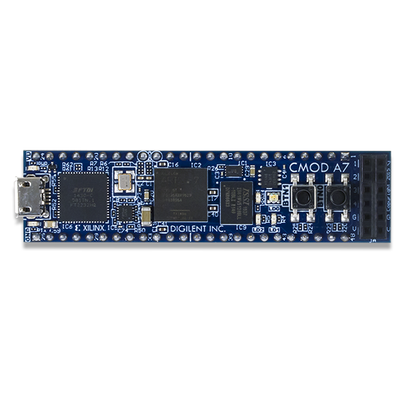
Key Features and Benefits
- One Pmod connector with 8 Digital I/O
- 48-pin DIP connector with 44 Digital I/O and 2 Analog inputs (0-3.3V)
- 2 Push Buttons
- 1 RGB LED
- 2 LEDs
- USB-UART bridge
- Powered from USB or external 3.3-5.5V supply connected to DIP pins
- USB-JTAG Programming Circuitry
- 4MB Quad-SPI Flash
- 512KB SRAM with an 8-bit bus and 8ns access times
- 5 clock management tiles
- 225 KB Block RAM
- 41,600 Flip-flops
- 20,800 LUTs
- Quad-SPI Flash/JTAG programming options
- 1 MSPS On-chip ADC
- FPGA: XC7A35T-1CPG236C
Документация по работе с платой
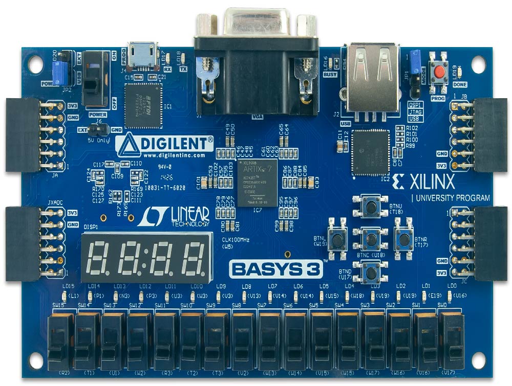
Key Features and Benefits
- 4 Pmod ports: 3 Standard 12-pin Pmod ports, 1 dual purpose XADC signal / standard Pmod port
- 4-digit 7-segment display
- 5 user pushbuttons
- 16 user LEDs
- 16 user switches
- USB HID Host for mice, keyboards and memory sticks
- 12-bit VGA output
- USB-UART Bridge
- Serial Flash
- Free WebPACK™ download for standard use.
- Designed Exclusively for Vivado Design Suite. Expanded features are available through purchase of the Design Edition.
- Digilent USB-JTAG port for FPGA programming and communication
- On-chip analog-to-digital converter (XADC)
- Internal clock speeds exceeding 450 MHz
- 90 DSP slices
- Five clock management tiles, each with a phase-locked loop (PLL)
- 1,800 Kbits of fast block RAM
- 33,280 logic cells in 5200 slices (each slice contains four 6-input LUTs and 8 flip-flops)
- Features the Xilinx Artix-7 FPGA: XC7A35T-1CPG236C
Документация по работе с платой
![]()
Нашли опечатку?
Выделите её, нажмите Ctrl+Enter и отправьте нам уведомление. Спасибо за участие!
Сервис предназначен только для отправки сообщений об орфографических и пунктуационных ошибках.